1
/
of
2
BuildYourCNC
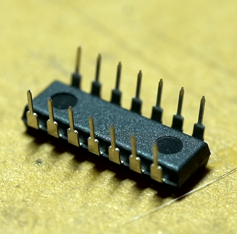
Quad Buffer Line Driver 74HC126E 14-Pin DIP
Quad Buffer Line Driver 74HC126E 14-Pin DIP
Regular price
$0.69 USD
Regular price
Sale price
$0.69 USD
Unit price
/
per
Couldn't load pickup availability
The 74HC126E is a quad non-inverting buffer/line driver IC in a 14-pin DIP (Dual In-line Package) format, part of the 74HC (High-speed CMOS) family. Here are its key characteristics:
- Operating Voltage: 2V to 6V typical, optimized for 5V operation
- Features four independent non-inverting buffers with 3-state outputs
- Each buffer has a separate output enable (OE) control pin
- Active-high enable inputs (output is enabled when OE is HIGH)
- High noise immunity characteristic of CMOS devices
- Propagation delay: typically 7ns at VCC = 5V
- Output drive capability: ±4mA at 5V
- Input levels compatible with both CMOS and TTL devices
Pin configuration (14-pin DIP):
- 1OE (Output Enable 1)
- 1A (Input 1)
- 1Y (Output 1)
- 2OE (Output Enable 2)
- 2A (Input 2)
- 2Y (Output 2)
- GND (Ground)
- 3Y (Output 3)
- 3A (Input 3)
- 3OE (Output Enable 3)
- 4Y (Output 4)
- 4A (Input 4)
- 4OE (Output Enable 4)
- VCC (Power Supply)
Common applications include:
- Bus interfacing
- Level translation
- Line driving for longer PCB traces
- Signal buffering between different logic families
- Data transmission in digital systems
74HC126E Quad Buffer Tutorial
What You'll Need
- 74HC126E IC
- 5V power supply
- Breadboard
- Jumper wires
- LEDs with current-limiting resistors (330Ω recommended)
- Push buttons or switches
- Pull-down resistors (10kΩ)
- 0.1µF bypass capacitor
Initial Setup
- Position the 74HC126E on your breadboard across the center gap
- Connect pin 7 (GND) to ground rail
- Connect pin 14 (VCC) to 5V supply rail
- Install a 0.1µF bypass capacitor between VCC and GND near the IC
Basic Buffer Operation
Testing Buffer 1:
- Pin 1: Output Enable (1OE)
- Pin 2: Input (1A)
- Pin 3: Output (1Y)
Basic Circuit Setup:
- Connect a 10kΩ pull-down resistor from Input pin (Pin 2) to ground
- Install a push button between 5V and the Input pin
- Connect the Output Enable pin (Pin 1) to 5V
- Connect an LED and 330Ω resistor from Output pin (Pin 3) to ground
How It Works
When you press the button:
- Input pin receives 5V (HIGH)
- Buffer activates (Output Enable is HIGH)
- Output follows input, lighting the LED
- Releasing the button returns output to LOW
Common Applications
1. Level Translation
Perfect for connecting 5V devices to 3.3V systems
2. Fan-out Expansion
Drive multiple devices from a single source
3. Bus Buffering
Isolate and protect sensitive circuits
Troubleshooting Tips
- Always use bypass capacitors for stable operation
- Keep voltage below 6V maximum
- Check Output Enable pins if output isn't working
- Verify all power and ground connections
- Consider using pull-up/down resistors for long connections
Technical Specifications
- Operating Voltage: 2V to 6V
- Optimized for 5V operation
- Four independent non-inverting buffers
- Individual output enable controls
- Compatible with both CMOS and TTL devices
Share


